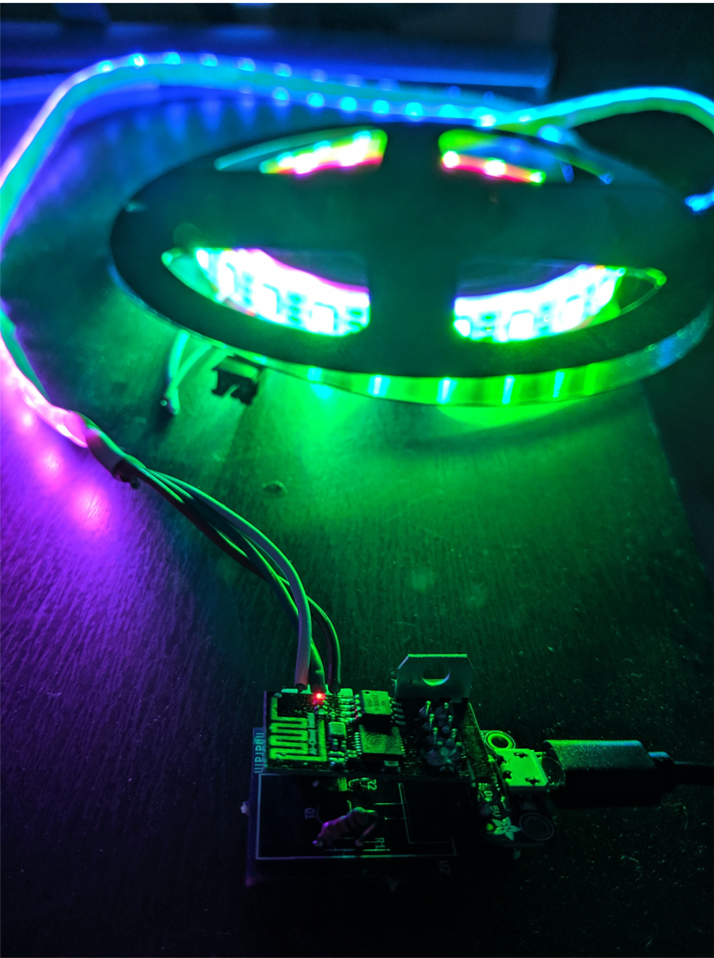
This project is an ESP8266 based light strip controller to be used as controllable accent lights for my house.
Basically what I wanted to achieve here was a device running custom firmware that I can control from my home automation system.
Hardware Design
First thing to do is decide what kind of hardware is going to be used for this project. So I need to define exactly what I need.
I know I want RGB lighting so the obivious choice for that is the very common WS2812b RGB LED light strip.
The choice for the microcontroller also came pretty quick as well. I need wireless connectivity and only a single GPIO pin to driver the light strip. The ESP8266 is an inexpensive WiFi chip that would great for this application, the specific SOC I’m using is the ESP-01 (Two GPIO pins and about $1 USD).
Ok. So that I know the core pieces I need to build my application. I need to figure out how to interface everything together.
- Obiviously I need a voltage source to power the device
- The ESP8266 is a 3.3V chip
- The WS2812B needs 5V, meaning I need two voltage sources on the board (5V and 3.3V)
- The 3.3V ESP device needs to interface with the 5V light strip circuit. So level shifting the data signal is required.
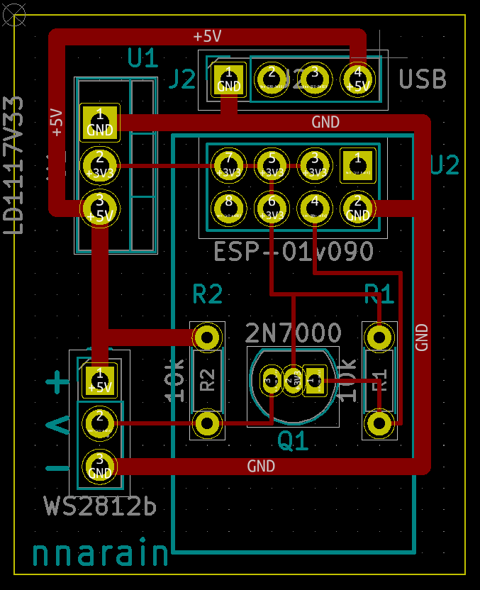
The following schematic was created in KiCAD.
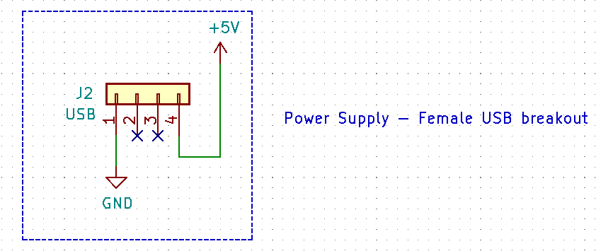
Power supply
For the power supply I was planning on using a common 5V USB phone charger. The power input to the device is then simply a Micro-USB breakout.
On the schematic it look like:
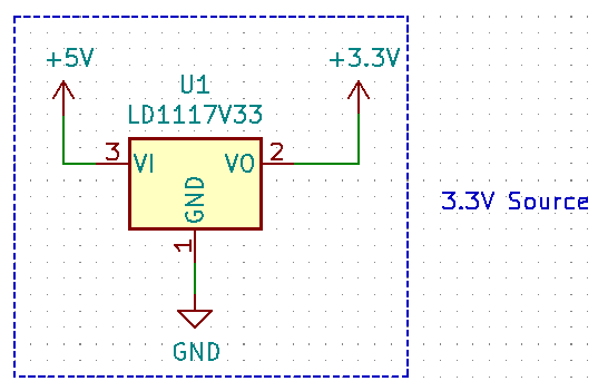
3.3V Source
As mentioned above a 3.3V source is required to power the ESP board. Here I simple use a 3.3V linear regulator
ESP-01
Below in the ESP-01 pin out.
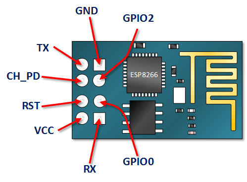
- In this application the serial communication is not used (it is used during development)
- Chip enable (CH_PD) is alway HIGH
- Reset (RST) is always HIGH
The ESP8266 has several boot modes configured by GPIO0 and GPIO2. For that we can refer to the following table. (GPIO15 is N/A in this case).
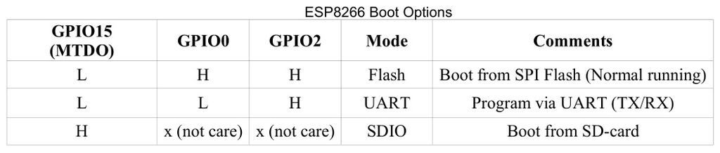
A normal boot requires both GPIO0 and GPIO2 to be pull HIGH.
Given all that information this is ESP-01 part of the schematic.
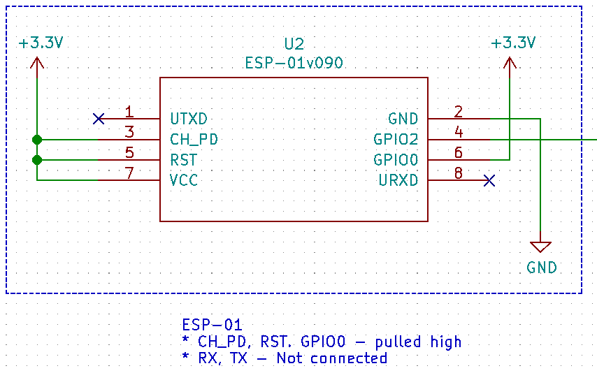
GPIO2 is also going to be used as the data signal for the LED strip and is pull HIGH (visible in the next diagram).
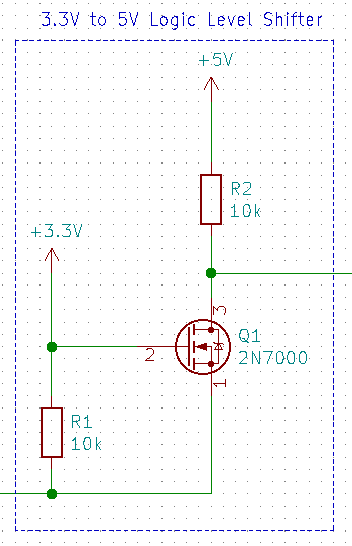
Level shifting circuit
To interface with the 5V part of the circuit and level shifting circuit is required. See below:
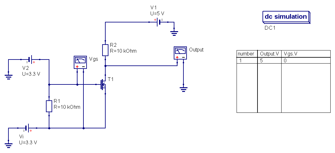
The input is V1.
When the input voltage is 3.3 V the gate-source voltage difference is 0, this causes the output to be pulled up to 3.3 V through R2.
When the input voltage is 0 V the gate voltage is pulled LOW, resulting in a gate-source voltage of 3.3 V. This allows the current to flow through the MOSFET,resulting in a output voltage of 0V.
Light strip connection
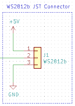
Simple 3 pin connector for the LED strip.
Prototyping
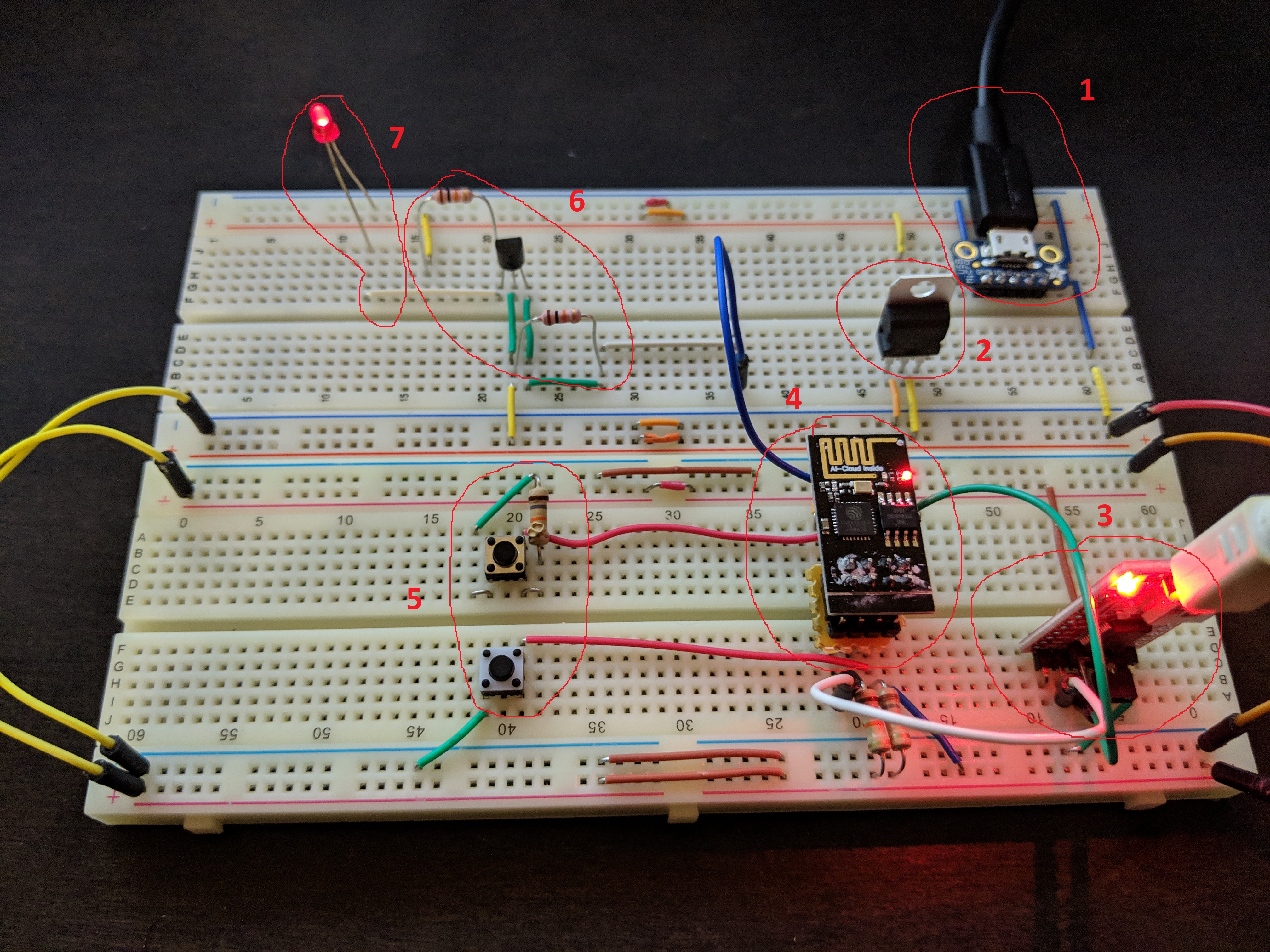
- USB input
- 3.3V linear regulator
- FTDI breakout (for programming over serial)
- The ESP-01 device
- Buttons to reset and enter flashing mode
- Level shifting circuit
- Output represened by an LED
Firmware
The next thing to do is to write to firmware and test it out on the breadboarded circuit.
Scope
Ok, so what exactly does the firmware need to do? I need it to connect to my home network, and be commandable by my home automation system.
This means that is needs to connect to WiFi, connect to the MQTT broker on my server and except JSON light commands (specified here).
Also, the device has to support persistant configuration for WIFI network, MQTT broker, number of LEDs on the strip, etc. This is so that it can recover from a power cycle.
Technically this information could be hard coded by that’s not good practice.
Since the device needs to be configured before it can connect to the WiFi network, I am using an AT command interface to configure the device over the serial port.
For example to configure the WiFi the following can be sent over the serial port.
AT+WIFI-MyWifi,MyWifiPassword
MQTT Config:
AT+MQTT-192.168.0.10,1883,/home/lights/esplight
Setting the LED count:
AT+LEDS-60
All the firmware was tested on the breadboard before ordering the PCB.
PCB
Layout
The ESP-01 is going to sit in a 4x2 socket, so it if elevated slightly, leaving room for the MOSFET and resistors to sit in the footprint of the ESP-01.
Also, due to the higher current going through the 5V rails I decided to make traces wider.
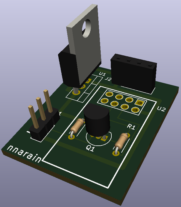
In the future I’d probably spend more time on the 3D model especially if it was going in an enclosure.
Also I’d like to make a logo for myself I can stick in a kicad library and throw on my future boards.
Board Fabrication
I decided to go with OSH Park. Getting the PCBs fabricated is incredibly easy apparently (not just with OSH Park but other companies as well). All I had to do was export my KiCAD files, generate the gerber files (drill files) and upload a zip to OSH park.
You do need to remember to check the design constrainsts of the manufacturer who to producing the boards. These boards are very simple so I didn’t have to change any of the KiCAD defaults.
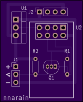
Here is the preview from the OSH site.
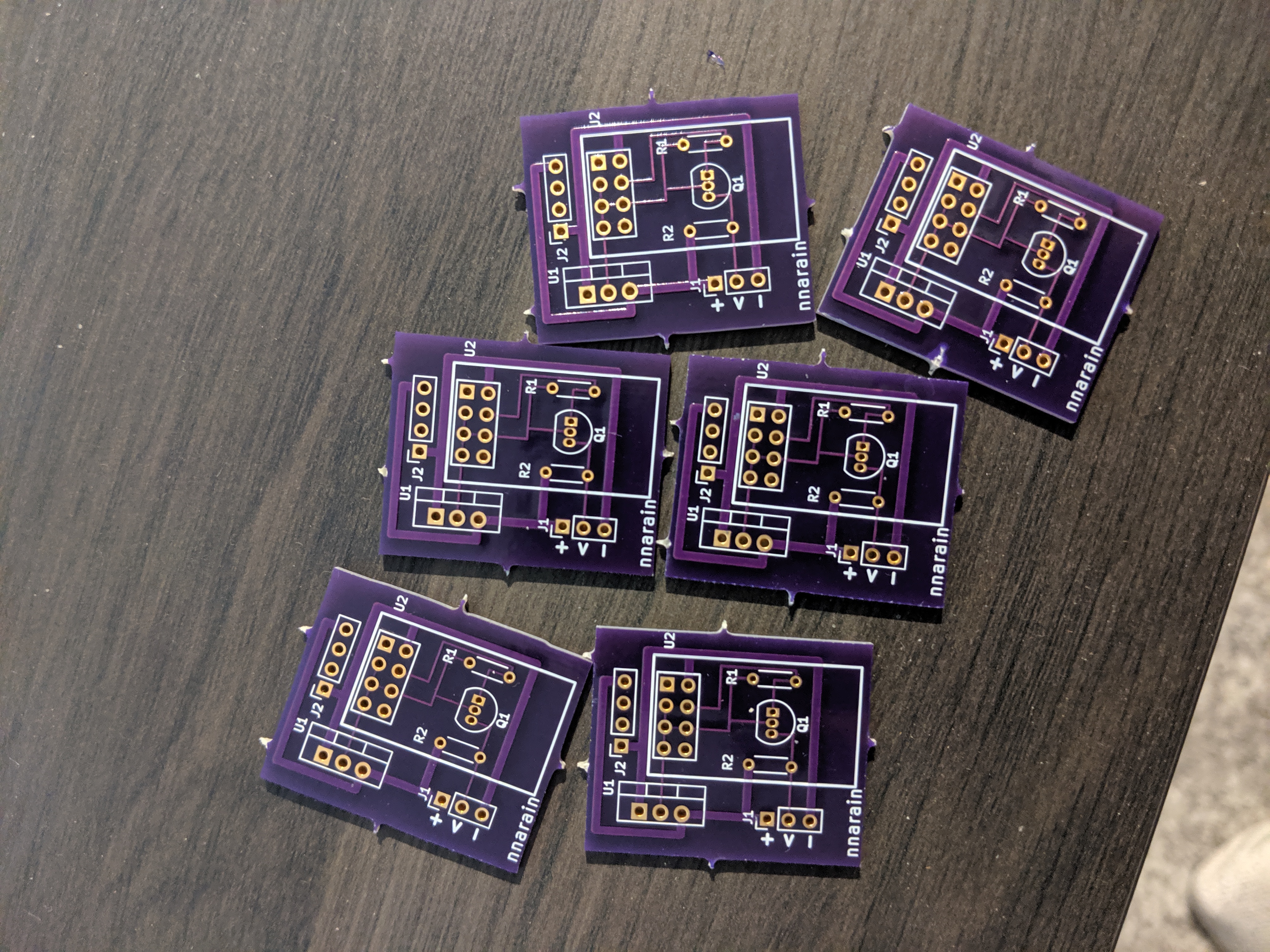
And the finished boards. Time from submission to delivery was 3 weeks (what OSH park estimated it would be).
Very cool and extremely satisfying to have an actual PCB.
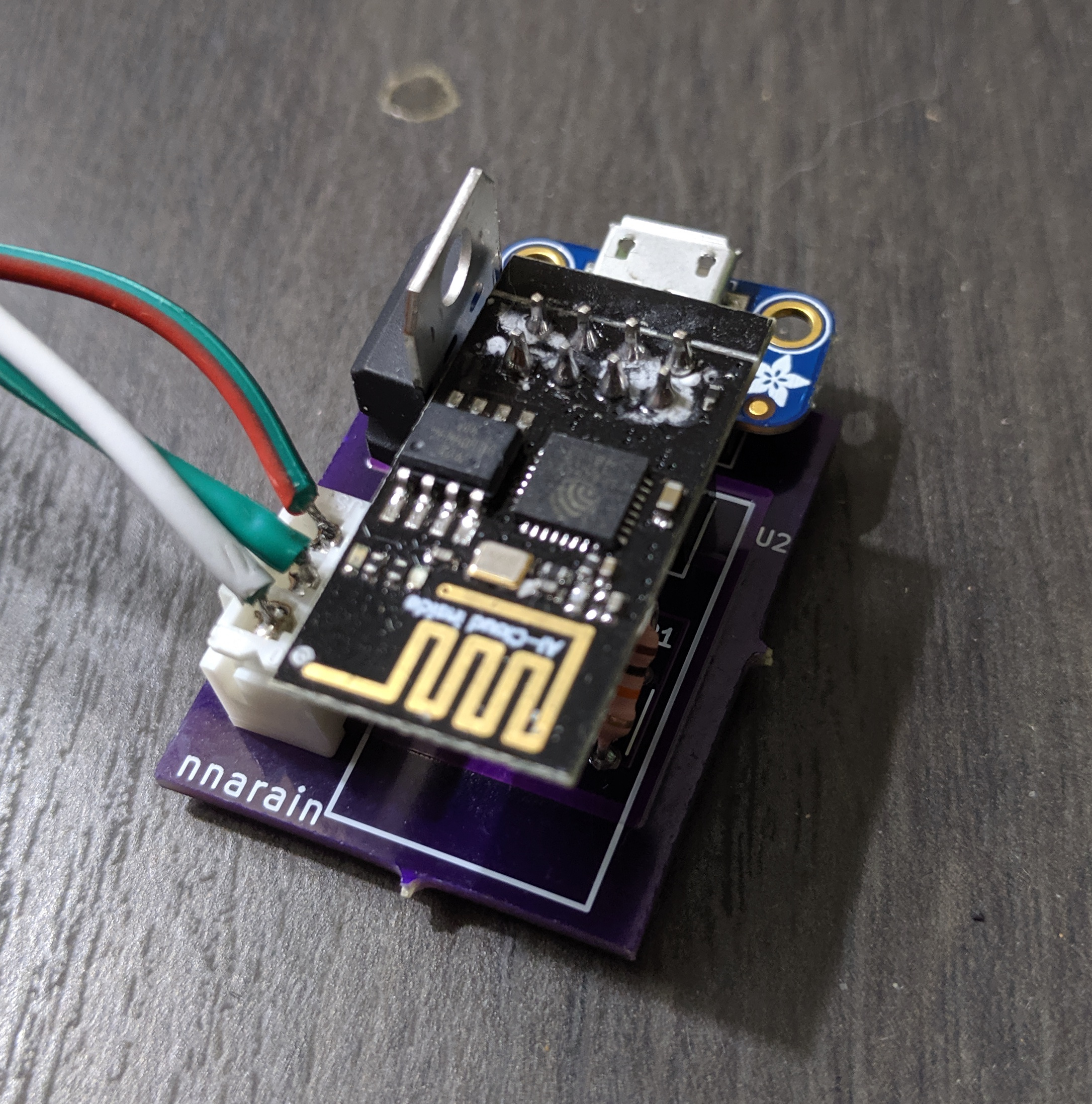
Board Assembly
Assembling the board is straight forward. Just need to solder in the components. I’ve always found making connectors a little fussy, but at the end of the day, not to bad!
Future
- Having a board printed was surprisingly cheap. So I’ll definitively doing a PCB for any electronics project down the line
- I was thinking about creating a programmer for the ESP-01 (Buttons for reset and flash, maybe onboard FTDI.). And make it a surface mount board to practice in that area.
1 post references this page